Power semiconductor
GaN + SiC device
| Main characteristics | Applying Effect | |
|---|---|---|
| GaN / SiC material properties |
|
|
| GaN+SiC Power device characteristics |
|
|
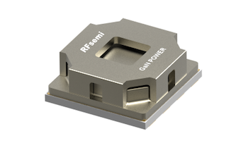
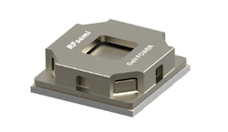
| RFsemi Power Package |
|
|
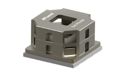
VSHS* : Variable Stack Heat Sink Package
- RFsemi Securing original patent
- Stacked Heat Sink Package
-
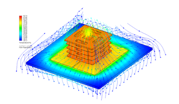
Chimney effect heat dissipation(VSHS)
-

VSHS Power package
GaN+SiC Modular Power Device
It consists of RFsemi's modular power devices using GaN and SiC. It has the following characteristics by utilizing the 'laminated heat sink package' applied for a patent as an independent technology.
1. Realization of miniaturization and high efficiency through world-class heat dissipation characteristics
2. High-speed switching through low-resistance/low-inductance implementation
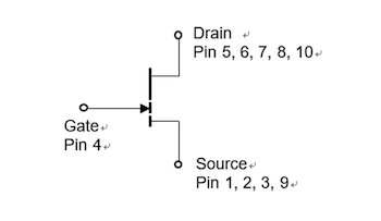
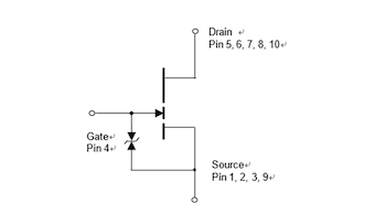
| GaN Power device | GaN Power device + Gate protection circuit | GaN Power device + Gate protection circuit + Boost SiC SBD |
|---|---|---|
 |
 |
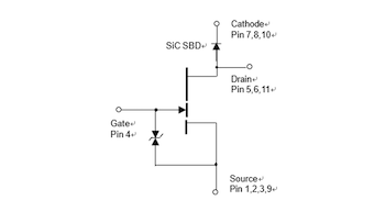 |
GaN Power device product line
| Part Number. | Configuration | VDS (V) | RDS_ON (mW) | QG (nC) | ID (A) | Status |
|---|---|---|---|---|---|---|
| RP10G73A | Single E GaN | 100 | 73 | 0.7 | 1.7 | Developing |
| RP10G30A | Single E GaN | 100 | 30 | 1.6 | 6 | Developing |
| RP10G15A | Single E GaN | 100 | 15 | 3.5 | 8 | Developing |
| RP10G7A | Single E GaN | 100 | 7 | 6 | 16 | Development Completed |
| RP10G4A | Single E GaN | 100 | 4 | 10.5 | 60 | Developing |
| RP65G450A | Single E GaN | 650 | 450 | 0.8 | 4 | Developing |
| RP65G200A | Single E GaN | 650 | 200 | 1.6 | 8 | Developing |
| RG65G150A | Single E GaN | 650 | 150 | 2.2 | 11 | Development Completed |
| RP65G100A | Single E GaN | 650 | 100 | 3.3 | 15 | Developing |
| RP65G67A | Single E GaN | 650 | 67 | 4.5 | 22 | Developing |
| Variable Stacked Heat Sink Package | |||
|---|---|---|---|
 |
 |
 |
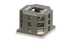 |
| HS0 | HS1 | HS2 | HS3 |
| 8X8X1.7 (mm) | 8X8X2.7 (mm) | 8X8X4.4 (mm) | 8X8X6.1 (mm) |
![]()
News
Warning: unlink(/home/rfsemi/public_html/en/data/cache/latest-notice-basic-3-23-f9db2c.php) [function.unlink]: Permission denied in /home/rfsemi/public_html/en/lib/Cache/FileCache.class.php on line 83
-
[공고] 권리주주 확정 기준일 설정인기글 관리자 08-04