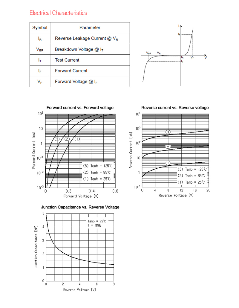
Product Description
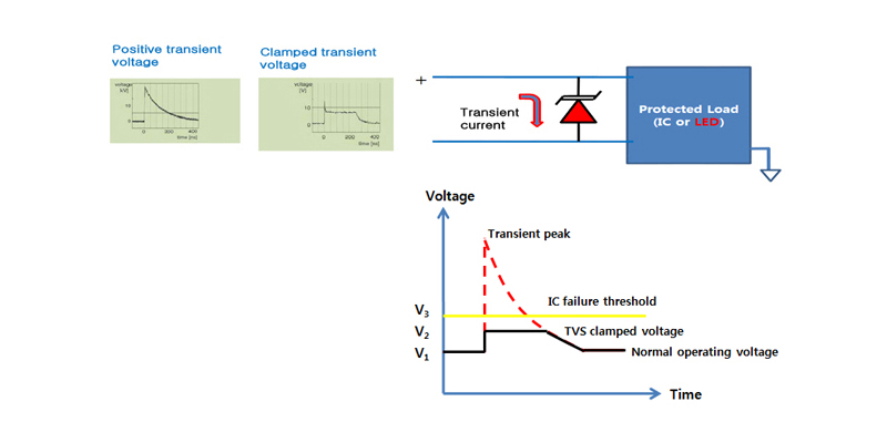
The Transient Voltage Suppressor (TVS) diode is a device that protects electronic circuits from over-voltage, and is widely applied to consumer electronics, computing devices, communications, and automotive applications, including portable devices.
RFsmi's TVS Diode is characterized by low clamping voltage and low leakage current and consists of a wide range of products, including power stage protection, battery terminal protection, Ear Micro, and speaker protection TVS diodes for ultra-fast data circuit protection, and reliability for ESD (IEC61000-4-2) and Surge (EC61000-561000-4I).
Product Structure
Applications
- SmartPhone
- Laptop
- Notebook, PC mainboard
- Sound and graphic card
Products
- General TVS Diodes
Part No Package PKG Standard PKG dimension
W x L x H (mm)Schmatic Vrwm(V) Vh Min(V) IR Max(㎂)
@VrwmVbr Min(V) Cj Max(pF) Ipp Max(A) VC Max(V) Remark RD1301 P-0806 SOD-923 1.0 x 0.6 x 0.4 
5 3.5 0.3 6 30 8 11 RD1301B P-0806 SOD-923 1.0 x 0.6 x 0.4 
5 5 0.25 5.5 20 5 10 RD1301BA P-0806 SOD-923 1.0 x 0.6 x 0.4 5 3 1 5.5 20 3 13 RDL1021 LLP1006 SOD-882 1.0 x 0.6 x 0.4 
5 3.5 1 6 35 7 13 RDL1031B LLP0603 0.62 x 0.32 x 0.25 
5 - 0.05 6 9 9 14 RDL1041B LLP1006 SOD-882 1.0 x 0.6 x 0.4 5 - 1 6 20 4 18 RDL1051B LLP1006 SOD-882 1.0 x 0.6 x 0.4 3.3 2.8 0.1 3.5 13 6 13 RDL1061B LLP1006 SOD-882 1.0 x 0.6 x 0.4 3.3 4.5 0.2 6 7 2 15 RDL1071B LLP1006 SOD-882 1.0 x 0.6 x 0.4 5 5 1 5.5 20 3 13 RDL1121B LLP0603 0.62 x 0.32 x 0.25 5 - 0.1 6 11 5 20 RDL1151B LLP1006 1.0 x 0.6 x 0.4 5 - 0.1 5.5 30 12 14 RDL1241B LLP1006 SOD-882 1.0 x 0.6 x 0.4 5 - 0.1 6 85 30 14 RDL1261 LLP1006 SOD-882 1.0x0.6x0.4 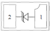
36 0.1 38 20 2.5 57 RDL1271 LLP1006 SOD-882 1.0 x 0.6 x 0.4 5.5 45 0.5 6.2 140 40 14 RDL1271B LLP1006 SOD-882 1.0 x 0.6 x 0.4 3.3 3.5 0.5 3.5 50 40 10 RDL1331B LLP0603 0.62 x 0.32 x 0.25 3.3 3.6 0.1 6 11 10 10 RDL1401 LLP1006 SOD-882 1.0x0.6x0.4 
10 0.1 11 150 20 20 RDP1011 P-080605 SOT-923 1.0 x 0.6 x 0.5 
5 - 1 6 20 5 18 RDP1051B P-080605 SOD-923 1.0 x 0.6 x 0.5 3.3 4 0.15 6 10 5 22 RDP1151B P-080604 SOD-923 1.0 x 0.6 x 0.4 5 0.1 5.5 30 12 14 - Low Cap TVS Diodes
Part No Package PKG Standard PKG dimension
W x L x H (mm)Schmatic Vrwm(V) Vh Min(V) IR Max(㎂)
@VrwmVbr Min(V) Cj Max(pF) Ipp Max(A) VC Max(V) Remark RDL1011B LLP1006 SOD-882 1.0 x 0.6 x 0.4 5 - 0.5 6 0.55 3 20 RDL1012 LLP1610 SLP1610P4 1.6 x 1.0 x 0.6 
5 - 1 6 0.8 1 15 Data line RDL1014 LLP2510 SLP2510P8 2.5 x 1.0 x 0.6 
5 - 1 6 0.8 1 17 Data line RDL1081 LLP1006 SOD-882 0.1 x 0.6 x 0.4 5 0.3 6 1 5 20 RDP1031 P-080605 SOD-923 1.0 x 0.6 x 0.5 5 - 0.5 6 0.55 3 20 RDP1081 P-080605 SOD-923 1.0 x 0.6 x 0.5 5 0.3 6 1 5 20 - PTVS(Power TVS) Diodes
Part No Package PKG Standard PKG dimension
W x L x H (mm)Schmatic Vrwm(V) IR Max(㎂)
@VrwmVbr Min(V) Cj Max(pF) Ipp Max(A) VC Max(V) Remark RDL3011 LLP1610D 1.6 x 1.0 x 0.6 
18 0.1 20 250 15 30 surge
waveform
8us/20usRDL3021 LLP1610D 1.6 x 1.0 x 0.6 26 0.1 28.5 - 13 42 surge
waveform
8us/20usRDL3031 LLP1610D 1.6 x 1.0 x 0.6 6 0.1 7 650 40 20 surge
waveform
8us/20usRDL3041 LLP1610D 1.6 x 1.0 x 0.6 5 0.1 6 300 25 18 surge
waveform
8us/20usRDL3051 LLP1610D 1.6 x 1.0 x 0.6 12 0.1 13 350 35 30 surge
waveform
8us/20usRDL3081 LLP2020B 2.0 × 2.0 × 0.6 
26 0.1 28 600 9.5 40 surge
waveform
10us/1000usRDL3221 LLP2020F 2.0 x 2.0 x 0.6 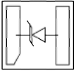
26 0.1 28 800 120 47 surge
waveform
8us/20usRDP3011 P-2617 SOD123W 3.5 x 1.7 x 0.7 
18 0.1 20 - 10 29.2 surge
waveform
10us/1000usRDP3021 P-2617 SOD123W 3.5 x 1.7 x 0.7 26 0.1 28.5 - 8.7 42 surge
waveform
10us/1000usRDP3031 P-1712A SOD-323F 2.5 × 1.2 × 0.7 6 0.1 7 650 40 20 surge
waveform
8us/20usRDP3041 P-1712A SOD-323F 2.5 × 1.2 × 0.7 5.5 0.2 6 300 25 18 surge
waveform
8us/20usRDP3051 P-1712A SOD-323F 2.5 × 1.2 × 0.7 12 0.1 13 350 35 30 surge
waveform
8us/20usRDP3101B P-1712A SOD-323F 2.5 × 1.2 × 0.7 4.5 0.5 5.2 250 84 22 surge
waveform
8us/20usRDP3111B P-1712A SOD-323F 2.5 × 1.2 × 0.7 4.5 0.5 4.6 210 80 20 surge
waveform
8us/20us - TVS Diode Array
Part No Package PKG Standard PKG dimension
W x L x H (mm)Schmatic Vrwm(V) Vh Min(V) IR Max(㎂)
@VrwmVbr Min(V) Cj Max(pF) Ipp Max(A) VC Max(V) Remark RD1305 P-1612 SOT-563 1.6 x 1.6 x 0.5 
5 3.5 1 6 40 8 13 Data line RD1305B P-1612 SOT-563 1.6 x 1.6 x 0.5 
3.5 3.5 0.1 5 15 5 12 RDL1015 LLP1610 SOT-886 1.6 x 1.0 x 0.6 
5 3.5 0.1 6 16 3 10 Data line RDL1022B LLP1006 SOD-882 1.0 x 0.6 x 0.4 
3.3 3.5 0.5 6 22 12 10 RDL1032 LLP1006C 1.0 x 0.6 x 0.4 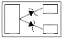
10 0.1 10.5 20 11.5 20 RDL1044B LLP1308 1.3 x 0.8 x 0.4 
3.3 3.5 0.1 4 10 9 10 Data line RDP1024 P-1612 SOT-563 1.6 x 1.6 x 0.5 
5 3.5 1 6 40 8 13 Data line RDP1024B P-1612 SOT-563 1.6 x 1.6 x 0.5 
3.5 3.5 0.5 5 15 5 12 Data line RDP1025B P-1612 SOT-563 1.6 x 1.6 x 0.5 
3.3 3.5 0.1 3.5 20 9.5 11
General Description
The zener diode is operating as a normal diode when forward biased, to the device to cause the zener breakdown current can increase rapidly in a particular voltage when reverse voltage is applied, the configuration of the constant voltage source less the change in the terminal voltage changes in the reverse current widespread is applied to.
Product Features
Applications
- Smartphone
- Laptop
- Headset / Earphone
- Digital Camera
List
| Part No | Package | PKG Standard | PKG dimension W x L x H (mm) |
Schematic | Vrwm(V) | IR Max(㎂) | Vbr Min(V) | Cj Max(pF) | Zener Impednace(Ω) | Remark |
|---|---|---|---|---|---|---|---|---|---|---|
| RDP2011 | P-0806 | SOD-923 | 1.0 x 0.6 x 0.4 |  |
10 | 1 | 11 | 25 | ||
| RDP2021 | P-0806 | SOD-923 | 1.0 x 0.6 x 0.4 | |
9 | 0.5 | 11.4 | 30 | - | |
| RDP2031 | P-1712A | SOD-323F | 2.5 x 1.2 x 0.7 | |
- | 5 | 5.2 | 275 | 7 | |
| RDP2041 | P-1712A | SOD-323F | 2.5 x 1.2 x 0.7 | 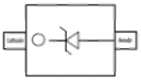 |
36 | 0.1 | 38 | 20 |
Product Description
General diode may be bonded o the P-type and N-type semiconductor, SBD is bonded to the metal and silicon.
Product Features
SBD is showing the same characteristics as the normal diode,but looking at the inside there is a great difference.
SBD is a UNI-Polar devices. So it is possible to operate in high speed. So it is easy to use in the high frequency region.
Product Features
Applications
- Smartphone
- Laptop
- Headset / Earphone
- Digital Camera
List
| Part No | Package | PKG Standard | PKG dimension W x L x H (mm) |
Schematic | IF (mA) | VF (V) | IR (㎂) | Vbr (V) | Cj Max (pF) | Remark |
|---|---|---|---|---|---|---|---|---|---|---|
| RDP4021 | P1712 | SOD-323F | 2.5 x 1.2 x 0.7 |  |
500 @ 0.5V | 0.27 @ 10mA | 150 @ VR=40V | 40 | 50 @ 1V | |
| RDP4031 | P1712 | SOD-323F | 2.5 x 1.2 x 0.7 | |
2000 @ 0.55V | 0.3 @ 100mA | 200 @ VR=20V | 20 | 60 @ 5V | |
| RRDP4011 | P-0806 | SOD-923 | 1.0 x 0.6 x 0.5 | |
25 @ 0.5V | 0.3 @ 2mA | 10 @ VR=10V | 20 | 5 @ 0.2V |
![]()
News
Warning: unlink(/home/rfsemi/public_html/en/data/cache/latest-notice-basic-3-23-f9db2c.php) [function.unlink]: Permission denied in /home/rfsemi/public_html/en/lib/Cache/FileCache.class.php on line 83
-
[공고] 권리주주 확정 기준일 설정인기글 관리자 08-04